1: Ultra-Clean Protection - Zero Wafer Contamination Constructed with semiconductor-grade PMMA material featuring ultra-low particle emission, compliant with high-class cleanroom standards. Ensures dust-free and scratch-free wafer surfaces to maximize production yield 2: Anti-Static Design - Protects Sensitive Circuits Rapid static dissipation effectively prevents electrostatic discharge (ESD) damage, making it ideal for high-precision semiconductor and microelectronics manufacturing 3: Industry-Leading Transparency - Enhanced Operational Efficiency Premium acrylic material with >92% light transmittance provides crystal-clear visibility of wafer surface defects and alignment marks. Significantly improves inspection/sorting efficiency while reducing manual handling 4: Impact-Resistant & Durable - Industrial-Grade Strength High-strength acrylic construction withstands impacts and chemical corrosion, with 5kg load capacity. Perfect for high-frequency transportation and stackable storage with minimal breakage risk 5: Ergonomic Design - Optimized Workflow Non-slip slots + beveled openings enable easy gloved operation. Stackable stand saves 60% storage space Product Details
Professional level wafer storage and transportation solution
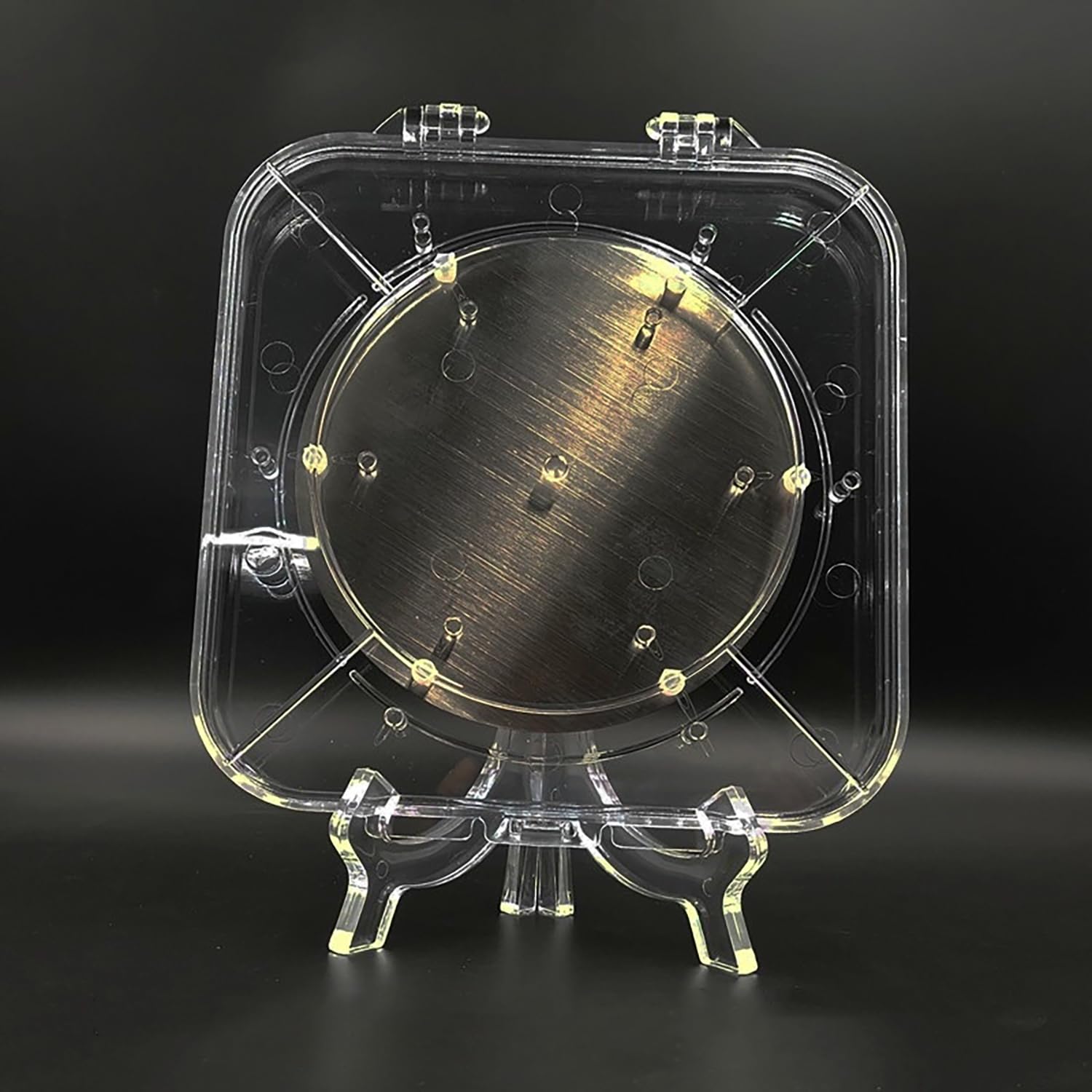
This high transparency monocrystalline carrier is designed specifically for 4-6 inch (152mm) semiconductor chips and is made of acrylic material, combining optical grade clarity with anti-static protection to ensure end-to-end safety from production to inspection.
Main functions
Visual wafer inspection: High transparency acrylic (transmittance ≥ 92%) allows for quick inspection of surface defects, alignment marks, and contamination without opening the lid, thereby improving inspection efficiency.
Double anti-static protection: The acrylic shell has a stable surface resistivity (10 ⁶~10 ⁹ Ω/sq), which can prevent damage to sensitive circuits.
Cleanroom ready: No degassing, no particles, zero pollution cleaning standards.
Industrial compatibility: inclined opening+anti slip groove, easy to handle with gloves.
Technical specifications
Material: Optical grade acrylic (PMMA)
Size: 170mm × 170mm × 25mm (applicable to standard 4-5-6 inch wafers)
Transmittance: ≥ 92%
Surface resistivity: 10 ⁶~10 ⁹ Ω/sq
Working temperature: -30 ° C to 80 ° C (short-term tolerance: 120 ° C)
Load capacity: 5kg
Key applications
Wafer Manufacturing: Temporary Storage/Transfer between Photolithography/Etching Processes
Inspection: Quick visual inspection or (automatic optical inspection) processing
R&D Laboratory: Protecting Experimental Semiconductor Samples
Packaging and testing: wafers during CP testing
Packaging and Scalability:
Including 1 wafer carrier and 1 detachable bracket
Up to 10 layers can be stacked to save clean room space
Professional level wafer storage and transportation solution
This high transparency monocrystalline carrier is designed specifically for 4-6 inch (152mm) semiconductor chips and is made of acrylic material, combining optical grade clarity with anti-static protection to ensure end-to-end safety from production to inspection.
Main functions
Visual wafer inspection: High transparency acrylic (transmittance ≥ 92%) allows for quick inspection of surface defects, alignment marks, and contamination without opening the lid, thereby improving inspection efficiency.
Double anti-static protection: The acrylic shell has a stable surface resistivity (10 ⁶~10 ⁹ Ω/sq), which can prevent damage to sensitive circuits.
Cleanroom ready: No degassing, no particles, zero pollution cleaning standards.
Industrial compatibility: inclined opening+anti slip groove, easy to handle with gloves.
Technical specifications
Material: Optical grade acrylic (PMMA)
Size: 170mm × 170mm × 25mm (applicable to standard 4-5-6 inch wafers)
Transmittance: ≥ 92%
Surface resistivity: 10 ⁶~10 ⁹ Ω/sq
Working temperature: -30 ° C to 80 ° C (short-term tolerance: 120 ° C)
Load capacity: 5kg
Key applications
Wafer Manufacturing: Temporary Storage/Transfer between Photolithography/Etching Processes
Inspection: Quick visual inspection or (automatic optical inspection) processing
R&D Laboratory: Protecting Experimental Semiconductor Samples
Packaging and testing: wafers during CP testing
Packaging and Scalability:
Including 1 wafer carrier and 1 detachable bracket
Up to 10 layers can be stacked to save clean room space